Discoveries and early devices

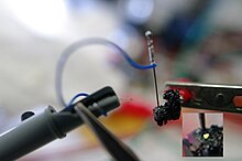
Green electroluminescence from a point contact on a crystal of SiC recreates H. J. Round's original experiment from 1907.
In 1961 American experimenters James R. Biard and Gary Pittman, working at Texas Instrument,[17] found that GaAs emitted infrared radiation when electric current was applied. The two were able to establish the priority of their work based on engineering notebooks, and received the first US patent for the LED (although the light emitted was infrared).
The first practical visible-spectrum (red) LED was developed in 1962 by Nick Holonyak, Jr., while working at General Electric Company.[8] Holonyak first reported this breakthrough in the journal Applied Physics Letters on the December 1, 1962.[18] Holonyak is seen as the "father of the light-emitting diode".[19] M. George Craford,[20] a former graduate student of Holonyak, invented the first yellow LED and improved the brightness of red and red-orange LEDs by a factor of ten in 1972.[21] In 1976, T. P. Pearsall created the first high-brightness, high-efficiency LEDs for optical fiber telecommunications by inventing new semiconductor materials specifically adapted to optical fiber transmission wavelengths.[22]
Commercial development
The first commercial LEDs were commonly used as replacements for incandescent and neon indicator lamps, and in seven-segment displays,[23] first in expensive equipment such as laboratory and electronics test equipment, then later in such appliances as TVs, radios, telephones, calculators, and even watches (see list of signal uses). Until 1968, visible and infrared LEDs were extremely costly, in the order of US$200 per unit, and so had little practical use.[6] The Monsanto Company was the first organization to mass-produce visible LEDs, using gallium arsenide phosphide (GaAsP) in 1968 to produce red LEDs suitable for indicators.[6] Hewlett Packard (HP) introduced LEDs in 1968, initially using GaAsP supplied by Monsanto. These red LEDs were bright enough only for use as indicators, as the light output was not enough to illuminate an area. Readouts in calculators were so small that plastic lenses were built over each digit to make them legible. Later, other colors became widely available and appeared in appliances and equipment. In the 1970s commercially successful LED devices at less than five cents each were produced by Fairchild Optoelectronics. These devices employed compound semiconductor chips fabricated with the planar process invented by Dr. Jean Hoerni at Fairchild Semiconductor.[24][25] The combination of planar processing for chip fabrication and innovative packaging methods enabled the team at Fairchild led by optoelectronics pioneer Thomas Brandt to achieve the needed cost reductions.[26] These methods continue to be used by LED producers.[27]
LED display of a TI-30 scientific calculator (ca. 1978), which uses plastic lenses to increase the visible digit size
Most LEDs were made in the very common 5 mm T1¾ and 3 mm T1 packages, but with rising power output, it has grown increasingly necessary to shed excess heat to maintain reliability,[30] so more complex packages have been adapted for efficient heat dissipation. Packages for state-of-the-art high-power LEDs bear little resemblance to early LEDs.
The blue and white LED

Illustration of Haitz's law. Light output per LED as a function of production year, with a logarithmic scale on the vertical axis
3Al
5O
12:Ce, or "YAG", phosphor coating to mix down-converted yellow light with blue to produce light that appears white. Nakamura was awarded the 2006 Millennium Technology Prize for his invention.[32]
The development of LED technology has caused their efficiency and light output to rise exponentially, with a doubling occurring approximately every 36 months since the 1960s, in a way similar to Moore's law. This trend is generally attributed to the parallel development of other semiconductor technologies and advances in optics and material science, and has been called Haitz's law after Dr. Roland Haitz.[33]
In 2001[34] and 2002,[35] processes for growing gallium nitride (GaN) LEDs on silicon were successfully demonstrated. In January 2012, Osram demonstrated high-power InGaN LEDs grown on Silicon substrates commercially.[36] It has been speculated that the use of six-inch silicon wafers instead of two-inch sapphire wafers and epitaxy manufacturing processes could reduce production costs by up to 90%.[37]


.jpg)


0 komentar:
Post a Comment